

- Posted on 17 Mar 2014
- 4-minute read
Silicon carbide is a semiconductor that is now widely used in a variety of micro-electromechanical systems, light-emitting diodes and high-power electronics. Its technological appeal stems from the fact that it is amenable to mature, robust nanofabrication methodologies and possesses both a high Young’s modulus and excellent thermal conductivity. To many, silicon carbide is a material that offers few surprises. Nevertheless, the increasing need for novel materials for implementing quantum technologies and nanophotonic integrated circuits is forcing scientists to revisit several traditional materials — silicon carbide is one of them.
The crucial step in manipulating a material in the quantum regime is the ability to modify and probe individual quantum states, which can be employed as qubits. Thus far, only diamond has offered a solid-state platform for optically stable, room-temperature single quantum emitters. The game has changed now, with works by Stefania Castelletto et al. and Hannes Kraus et al. who have isolated single emitters and identified microwave spin qubits in silicon carbide.
Castelletto et al., who report their results in Nature Materials, identified individual defects, known as carbon anti-site vacancy pairs, in silicon carbide that are sufficiently bright to allow detection at the single-photon level. These emitters can generate single photons at a high repetition rate, which makes them potentially useful qubits for quantum information processing and applications in photonics. The defects have the practical benefit that they are optically active at room temperature. Another notable advantage is their natural abundance in the host matrix. Consequently, there is no need for external ion implantation, as in the case of diamond, or for the cumbersome epitaxial growth typical of III–V semiconductors. Electron irradiation and annealing provide the material restructuring needed to optically activate the defects. It is thought that the defects are clusters comprising carbon atoms that reside in silicon sites adjacent to carbon vacancies.
In a parallel report in Nature Physics, Kraus et al. describe optically induced population inversion of the spin states of another type of single defect in silicon carbide — a silicon vacancy. This critical result paves the way to silicon carbide solid-state masers and extremely sensitive travelling-microwave amplifiers. Moreover, by exploiting the double radio optical resonance technique, the team unambiguously proved that the silicon vacancy has a spin-3/2 ground state — a topic that has been under debate for many years. They are therefore able to detect an optical magnetic-resonance signature from a silicon-vacancy defect at room temperature. The ability to focus exclusively on a known defect at room temperature in a forest of paramagnetic centres is crucial for practical and scalable engineering of sensors and solid-state devices for quantum information processing.
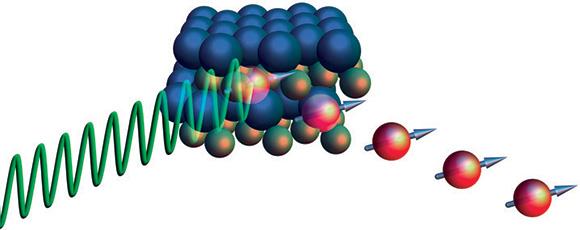
Figure 1
So, despite many years of intense research on silicon carbide and its spectroscopic characterisation, why have single-photon emission and unambiguous identification of paramagnetic defects not been previously observed? The answer to this question is rather simple. In traditional semiconductor physics, most spectroscopy is performed using above-bandgap laser excitation that predominantly excites near-gap emissions. However, this approach cannot address deep-level states. Instead, individual defect states that reside within the forbidden energy gap must be optically accessed using sub-bandgap excitation. This is a critical issue for wide-bandgap semiconductors. Indeed, this is the case for the infamous negatively charged nitrogen-vacancy centre in diamond, which is visible on green excitation but inaccessible by ultraviolet excitation. Silicon carbide, not surprisingly, shows similar behaviour — red and infrared excitation, as was cleverly used by Castelletto, Kraus and their colleagues, is not sufficiently energetic to promote electrons into the conduction band, but provides an excellent way to identify new quantum systems at room temperature (Fig. 1). Both works highlight the urgent need to revisit other wide-bandgap materials, including zinc oxide and aluminium nitride. Surely, it will not be long before more robust room-temperature quantum systems are unveiled.
The pivotal observation of single-photon sources and stimulated microwave emission from silicon carbide complements the recent discovery of novel fluorescent silicon carbide nanostructures (tetrapods) and ushers in a new era for this technologically important material. Integration of single defects into nanomechanical systems will pave the way to the burgeoning field of optomechanics and enable unprecedented applications in sensing, quantum information processing and magnetometry. At last, we have a convincing candidate for scalable quantum devices at our fingertips.
Byline: Igor Aharonovich and Milos Toth